
Terafab: Elon Musk’s Joint Chip Initiative Unites Tesla, SpaceX and xAI Around an Austin Advanced-Technology Fab
Terafab, Elon Musk’s chip initiative for Tesla, SpaceX and xAI, plans an Austin advanced-technology fab to develop in-house AI and robotics semiconductors.
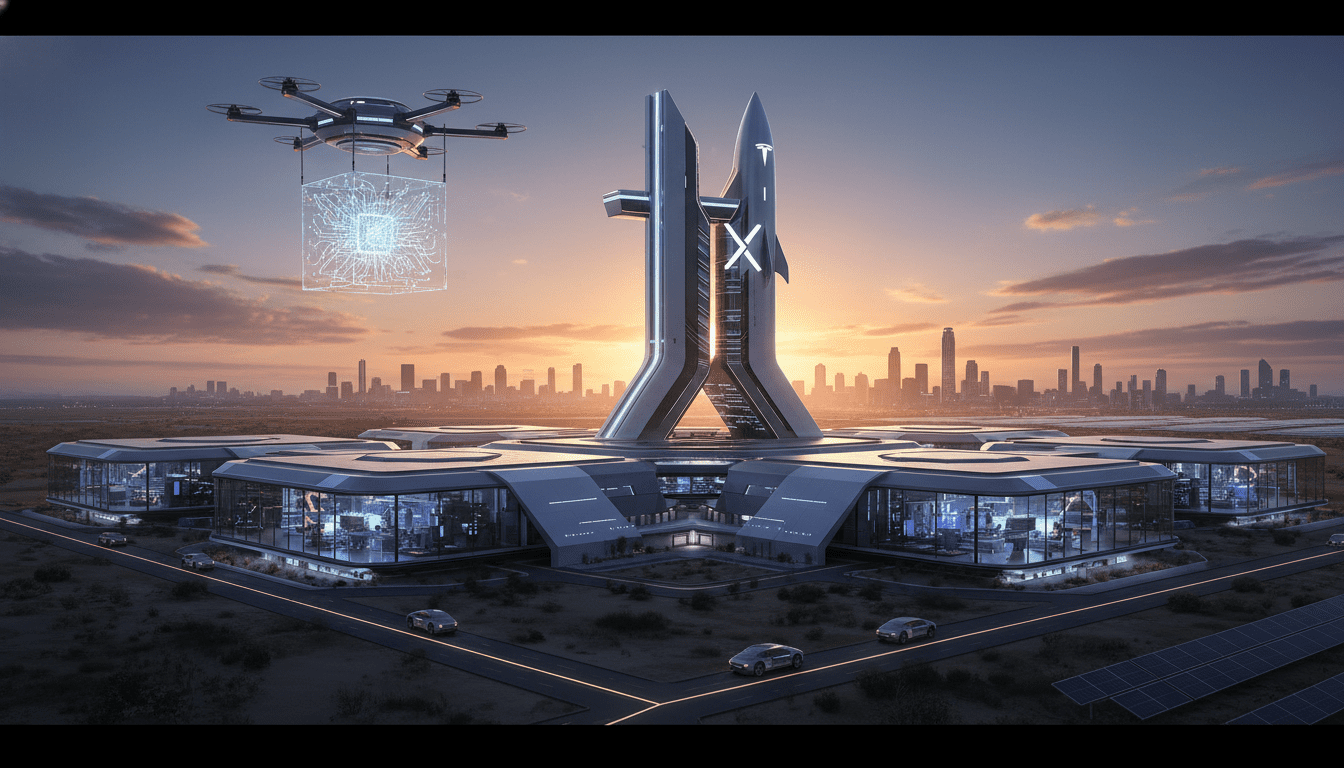
Elon Musk has announced Terafab, a coordinated semiconductor effort intended to serve Tesla, SpaceX and xAI, beginning with an advanced-technology facility in Austin, Texas. The move signals a push to internalize critical hardware for AI, robotics and space applications—areas that have become central to Musk’s businesses. Terafab is being described as an opening step: a design and test-oriented site rather than a full-volume foundry. That framing matters because it sets expectations about scope, timeline and the scale of investment required to turn a prototype-capable campus into a mass-production operation.


Terafab’s Austin Launch and Project Scope
Musk introduced Terafab as a multi-company semiconductor initiative centered initially in Austin, where a compact, advanced-technology facility will focus on chip design validation and test flows. According to public reporting, Tesla and SpaceX are slated to jointly operate the site with xAI tied into the program; the Austin location is explicitly described as the first move, not the final large-scale fabrication campus. In practice, that means the initial site will likely handle tasks common to early-stage fab work: design-for-manufacturability checks, test wafers, prototype runs and characterization of novel process flows that target compute for robotics, AI inference/training acceleration, and resilient systems for space environments.
Framing the project as a phased effort rather than a single monolithic plant is significant. A successful semiconductor strategy typically requires distinct facilities and investments for R&D, pilot production and high-volume manufacturing—each with different land, power and capital demands. Terafab’s Austin facility appears intended to sit at the front end of that continuum: giving Musk’s businesses closer control over chip architectures and early fabrication work while leaving open the question of where and when any large-scale production fabs would be built.
What Terafab Is Designed to Achieve
Terafab aims to do several interconnected things at once. First, it seeks to reduce dependence on external suppliers for specialized chips that power autonomous vehicles, general-purpose and custom AI models, robotics actuators and space-hardened compute systems. Second, by creating a shared pipeline across Tesla, SpaceX and xAI, the initiative intends to align hardware roadmaps with software and systems engineering efforts—shortening feedback loops between chip design and product integration. Third, it offers a locus for experimentation on chips tuned for robotics workloads, on-orbit data processing, and the high-throughput model inference that xAI demands.
How will this work in practice? The initial facility will likely focus on design verification, packaging prototypes, and test flows that validate performance, thermal characteristics and radiation tolerance where relevant. These outputs would then inform whether larger, dedicated fabrication capacity is needed elsewhere—capacity that requires major investments in land, electricity infrastructure and process engineering. Terafab’s early-stage approach positions it to iterate on architectures and validate manufacturability before committing to the immense capital expenditures of full-scale fabs.
Why does this matter? Semiconductors are now a strategic choke point across the most technology-intensive industries. For companies pursuing autonomy, advanced robotics and orbital services, tailor-made chips can materially improve latency, energy efficiency and long-term cost. Bringing more of that development in-house offers Musk’s companies potential gains in agility and differentiation—but also exposes them to the steep technical and financial challenges inherent in chip manufacturing.
How Tesla, SpaceX and xAI Fit Together Under Terafab
Each company in Musk’s ecosystem has distinct compute requirements that could benefit from a coordinated chip strategy. Tesla’s ambitions in autonomous driving and humanoid robotics emphasize low-latency, high-efficiency inference engines that can run on vehicles or edge robots with tightly constrained power and thermal envelopes. xAI’s platform needs large amounts of throughput for model training and tailored accelerators for inference workloads. SpaceX, meanwhile, has evolving interests in on-orbit processing, communications payloads and systems that must perform under radiation and extreme thermal conditions.
Terafab’s shared pipeline is intended to reconcile these diverse demands by enabling cross-pollination of design concepts—reusable IP blocks, packaging techniques and testing protocols—while allowing for specialization where requirements diverge. For instance, a neural-network accelerator developed for Tesla’s vehicle stack could be adapted with different radiation-hardened components or packaging for SpaceX payloads, while xAI could deploy scaled versions of the same architecture in datacenter racks. The organizational model suggested by the announcement implies joint governance over early-stage R&D and testing, with downstream manufacturing decisions tailored to each company’s volumes and reliability needs.
Technical, Operational and Financial Challenges of Building a Fab
Moving from prototype to production is fraught with hurdles. Semiconductor fabrication at scale requires not only capital but deep operational expertise, complex supply chains, and enormous utilities. Real-world fabs demand continuous flows of ultra-pure water, stable high-voltage power with significant redundancy, climate control, specialty chemicals and logistics that can handle sensitive wafers. In addition, process node mastery—lithography, etch, deposition and yield management—takes years of iterative manufacturing data and expert staff.
Cost is another major factor. Building and equipping a modern fab can require tens of billions of dollars depending on the target process node and output capacity. Land and power availability are critical: large multicampus fabs need vast physical footprints and grid upgrades or dedicated power generation. Permitting, local infrastructure and workforce development also influence where a high-volume plant can be economically sited. The initial Austin facility minimizes upfront exposure by focusing on advanced testing and proof-of-concept flows; however, any expansion into high-volume manufacturing would amplify these challenges.
Technical talent is a third constraint. Semiconductor production depends on seasoned process engineers, yield analysts, materials scientists and specialized technicians—skills that are not trivial to acquire at scale, particularly in regions without an existing semiconductor ecosystem. Developing this workforce can take years and often requires partnerships with universities, training programs and subcontractors.
Finally, there’s the knowledge gap: while Musk’s companies have strong track records in manufacturing automotive, rocket and software systems, large-scale silicon manufacturing is an entirely different discipline. Success will hinge on recruiting experienced chipFoundry operators, securing supplier relationships for key equipment and materials, and implementing stringent quality management systems.
Competitive and Industry Context Around Terafab
Terafab lands in a competitive and strategic environment where industry incumbents and hyperscalers are also expanding into specialized hardware. Companies like Nvidia have deep expertise in AI accelerators and are actively exploring space and edge compute architectures; the trend toward specialized AI silicon has attracted investments from cloud providers, chip startups and national initiatives aiming to bolster domestic semiconductor capacity. Orbital computing—the idea of deploying data centers or compute nodes in space—has also drawn attention from hardware vendors seeking to adapt chips to radiation-hardened, thermal-challenged environments.
Terafab’s emphasis on combining robotics, AI and space compute places it at the confluence of these trends. If fully developed, the program could offer differentiated hardware tuned to use-cases that existing players target with general-purpose accelerators. That said, incumbent foundries and chip designers have years of process mastery and scale that make competitive entry difficult. Terafab’s niche could lie in customized, vertically integrated solutions that prioritize co-design between silicon and system-level software, rather than trying to compete head-on with high-volume consumer or datacenter silicon suppliers.
Developer, Product and Business Implications
For software and systems engineers working at Tesla, SpaceX or xAI, Terafab could shorten iteration cycles between algorithm design and hardware validation. Access to custom accelerators or tailored packaging would let teams optimize models for specific energy-latency trade-offs and test them in realistic conditions. For robotics developers, bespoke ASICs or heterogeneous compute stacks could enable longer run times, denser sensor fusion, and improved control loops.
Product teams would need to account for a tighter hardware-software dependency: releasing new features could require synchronized silicon updates, firmware changes and supply-chain planning. That raises the bar for cross-functional coordination but also creates an opportunity for deeper integration and competitive differentiation. For customers and partners, a vertically integrated stack could mean faster innovation cycles but also potential vendor lock-in.
Businesses should weigh the trade-offs between owning critical hardware IP and the capital, time and operational complexity required to manufacture it. For companies that can successfully integrate custom silicon into product roadmaps, the benefits include optimized performance, reduced dependency on external suppliers and stronger margins on specialized systems. For others, the recommended approach may remain partnering with established chip vendors and using third-party foundries.
Supply Chain, Security and Policy Considerations
Terafab touches broader strategic issues around supply chain resilience and national policy. Recent years have underscored the fragility of global semiconductor supply lines and prompted governments to incentivize domestic manufacturing. A high-profile program that localizes critical chip development could align with industrial policy priorities—if it scales beyond prototyping and demonstrates job creation and infrastructure investment.
Security is another dimension. Designing and manufacturing key components in-house can reduce exposure to third-party supply-chain risks and intellectual property leakage. However, managing secure design flows and protecting IP across multiple entities in a joint program requires rigorous governance. For space applications, certification and radiation-hardening protocols add another layer of regulatory and safety scrutiny.
Economic Risks and the Realities of Vertical Integration
Vertical integration has been a hallmark of Musk’s approach across industries, from cars to rockets. Integrating semiconductor development into that strategy offers potential synergies—closer alignment of hardware and software roadmaps, tighter cost control and bespoke performance advantages. Yet the semiconductor industry’s economics are unforgiving: mistakes in process choice, underestimation of capital needs, or slow yield ramp-up can lead to years of negative returns.
Furthermore, the value of owning a foundry depends on volume and specialization. If Terafab’s chips are highly specialized for Musk’s internal products, a smaller-scale advanced fab might be economically defensible. But if the goal is to produce widely used AI accelerators at datacenter scale, competing with established foundries and design ecosystems will require orders of magnitude more investment.
Signals to Watch: How Terafab Might Evolve
Key indicators will reveal whether Terafab stays an R&D-focused operation or becomes the start of a larger manufacturing footprint. Watch for announcements about:
- Additional facility locations or land acquisitions indicating plans for high-volume fabs.
- Capital allocations and partnerships with equipment suppliers, which would signal movement toward production scale.
- Hiring drives that bring in experienced fab operators, process engineers and supply-chain specialists.
- Public disclosures of prototype silicon, performance benchmarks, or packaging innovations that validate Terafab’s technical trajectory.
- Regulatory filings, permitting activity or grid infrastructure investments around candidate sites beyond Austin.
Each of these actions would mark a step from experimental capability toward industrial-scale manufacturing.
Broader Industry Implications for Developers, Businesses and the Market
Terafab, even in its early form, is a reminder that hardware is again a strategic battleground. For developers and teams focused on AI, robotics or edge systems, greater availability of tailored silicon could unlock new product architectures and efficiency gains. For businesses, the initiative highlights two strategic choices: invest in vertical integration for tight control and differentiation, or leverage established ecosystems for scale and lower capital exposure.
At the market level, if Terafab or similar efforts succeed, we could see a wave of bespoke silicon tailored to narrow classes of workloads—robots, autonomous vehicles, or space-based compute—leading to more heterogeneous computing environments. That will drive demand for new developer tools, compilers, and performance-validation platforms that connect high-level models to specialized hardware.
Policy-makers and supply-chain managers will also take note. High-profile industrial initiatives can reshape regional economic development, create specialized talent hubs and influence national semiconductor strategies. Strategic investments in domestic semiconductor capabilities will likely continue, and private-sector initiatives like Terafab will be evaluated for their potential to accelerate or complement those public efforts.
Operational Scenarios and Business Use Cases
Practical scenarios where Terafab’s outputs could be deployed include: Tesla integrating energy-efficient inference chips into next-generation autopilot and humanoid robots; xAI deploying tailored accelerators across model training clusters to reduce power and cost per training cycle; and SpaceX outfitting satellites or orbital hubs with processors designed for high-throughput telemetry processing and resilience to space conditions. Each use case underscores different requirements—thermal management, compute density, radiation tolerance and lifecycle support—which a specialized pipeline can address more effectively than off-the-shelf chips.
For enterprise customers and partners, certification programs and performance guarantees will be essential if Terafab silicon is to be used in commercial offerings. That raises questions about manufacturing capacity, supply commitments, and long-term support—areas where careful contract design and ecosystem partnerships will be needed.
The early emphasis on an Austin test facility suggests that Musk’s companies intend to validate concepts before committing to larger-scale supply promises. This staged approach can be beneficial: it reduces initial exposure, allows rapid architectural experimentation, and provides empirical data to guide subsequent capital allocations.
There will also be opportunities for adjacent industries. Companies that supply packaging, thermal solutions, test equipment or materials may find new demand if Terafab scales. Similarly, universities and training programs in semiconductor engineering could see incentives to expand curricula and research collaborations.
Looking ahead, the development and scaling of Terafab will be a test case in blending software-driven product cycles with the long capital timelines of semiconductor manufacturing. If the program can effectively bridge the cadence mismatch—rapid model iterations on one hand and slow fab ramps on the other—it could serve as a model for other vertically integrated technology firms. Conversely, if capital intensity and operational complexity outweigh the strategic benefits, Terafab may remain a specialized R&D asset rather than a mass-production engine.
Regardless of the path, Terafab reframes a key question for the industry: how much hardware activity should technology companies internalize to maintain competitive advantage, and what is the optimal balance between in-house control and external partnership?
The next year will likely reveal whether Terafab remains an exploratory hub in Austin or becomes the nucleus of a broader manufacturing ecosystem; either outcome will influence how companies think about co-designing silicon, software and systems in a world where AI, robotics and space computing are increasingly intertwined.


